MT47H128M8SH-25E IT:M
DRAM, DDR2, 1 Gbit, 128M x 8bit, 400 MHz, TFBGA, 60 Pins
Bạn cần thêm?
| Số Lượng | Giá |
|---|---|
| 1+ | US$4.260 |
| 10+ | US$3.950 |
| 25+ | US$3.770 |
| 50+ | US$3.730 |
| 100+ | US$3.680 |
| 250+ | US$3.580 |
| 500+ | US$3.500 |
Thông Tin Sản Phẩm
Tổng Quan Sản Phẩm
MT47H128M8SH-25E IT:M is a DDR2 SDRAM. It uses a double data rate architecture to achieve high-speed operation. The double data rate architecture is essentially a 4n-prefetch architecture, with an interface designed to transfer two data words per clock cycle at the I/O balls. A single READ or WRITE operation for the DDR2 SDRAM effectively consists of a single 4n-bitwide, two-clock-cycle data transfer at the internal DRAM core and four corresponding n-bit-wide, one-half-clock-cycle data transfers at the I/O balls. A bidirectional data strobe (DQS, DQS#) is transmitted externally, along with data, for use in data capture at the receiver. DQS is a strobe transmitted by the DDR2 SDRAM during READs and by the memory controller during WRITEs. DQS is edge-aligned with data for READs and centre-aligned with data for WRITEs. The x16 offering has two data strobes, one for the lower byte (LDQS, LDQS#) and one for the upper byte (UDQS, UDQS#).
- 128M8 configuration, tCK = 2.5ns, CL = 5 cycle time
- JEDEC-standard 1.8V I/O (SSTL_18-compatible), differential data strobe (DQS, DQS#) option
- Programmable CAS latency (CL), posted CAS additive latency (AL)
- Selectable burst lengths (BL): 4 or 8, adjustable data-output drive strength
- DLL to align DQ and DQS transitions with CK, 8 internal banks for concurrent operation
- Industrial temperature range from -40°C to +85°C
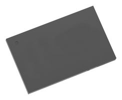
- Package style is 60-ball FBGA
Thông số kỹ thuật
DDR2
128M x 8bit
TFBGA
1.8V
-40°C
-
1Gbit
400MHz
60Pins
Surface Mount
95°C
Tài Liệu Kỹ Thuật (1)
Pháp Chế và Môi Trường
Quốc gia nơi quy trình sản xuất quan trọng cuối cùng được thực hiệnNước xuất xứ:China
Quốc gia nơi quy trình sản xuất quan trọng cuối cùng được thực hiện
RoHS
RoHS
Chứng Nhận Chất Lượng Sản Phẩm